SidecarTridge RP2M2
The SidecarTridge RP2M2 is a small microcontroller board built on the Raspberry Pi RP2350B, in the shape of an M.2 card. Its name stands for Raspberry Pico to M.2. It brings all 48 GPIO pins of the RP2350B to its gold edge connector, so one board can serve many designs: it plugs into a carrier board made for each computer.
It is the board on top of the SidecarTridge TOS Emulator and the SidecarTridge Kickstart Multi ROM, whose guides call it board revision 4 (RP2350B).
The current revision of the RP2M2 is revision 1.4.0, printed on the component side next to the RESET button as REV 1.4.0. That is the RP2M2’s own revision number. It is not the “board revision 4” of the TOS Emulator and Kickstart Multi ROM guides, which count the boards those products have had.
Table of contents
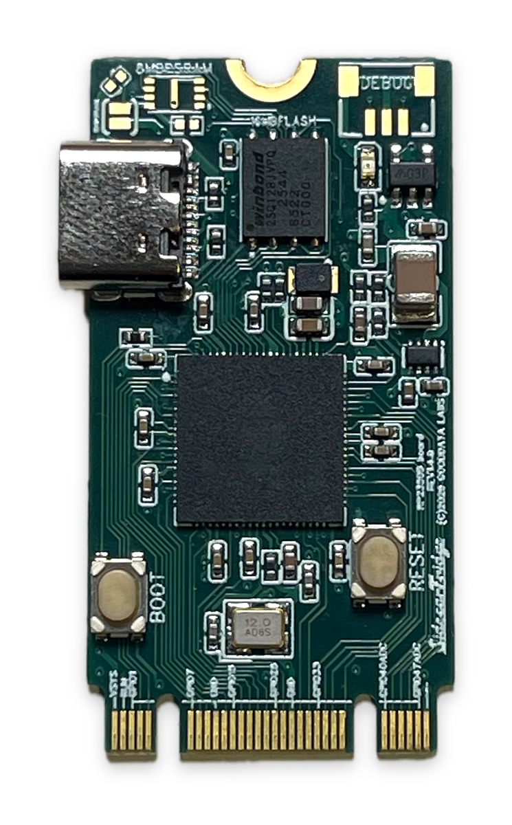
BOOT and RESET buttons, and the DEBUG pads at the top right.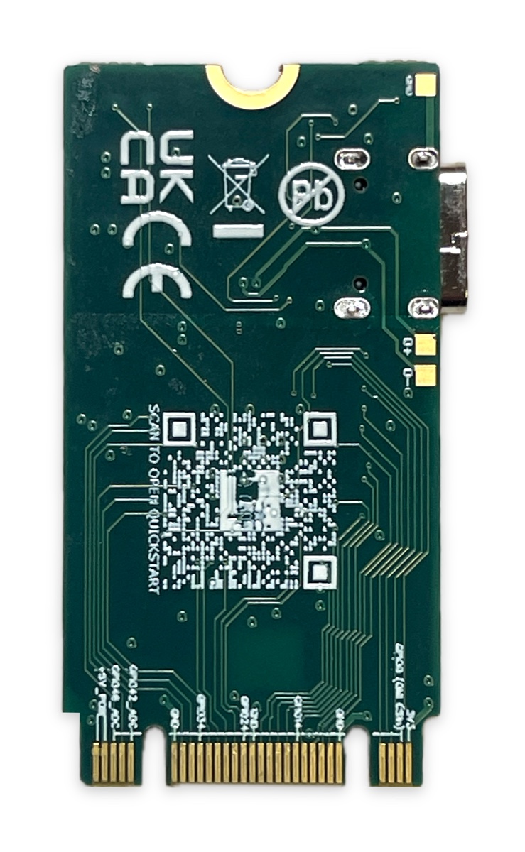
D+ and D- pads.The RP2M2 is not an M.2 device. It has the shape and the connector of an M.2 card, but its pins carry the GPIO pins of the microcontroller and a +5 V input, not the M.2 signals. Never plug it into the M.2 slot of a PC, a laptop or an SSD enclosure, and never plug an M.2 SSD or Wi-Fi card into a SidecarTridge carrier board: either can be damaged.
Versions
The RP2M2 comes in three versions. They differ in the memory and in the debug connector, and in nothing else: the microcontroller, the flash memory, the edge connector and its pins are the same in all three.
| Version | Flash memory | PSRAM | DEBUG connector |
|---|---|---|---|
| RP2M2 16MB Flash | 16 MB | No | Not fitted: pads only |
| RP2M2 16MB Flash + 8MB PSRAM | 16 MB | 8 MB | Not fitted: pads only |
| RP2M2 16MB Flash + 8MB PSRAM + DBG connector | 16 MB | 8 MB | Fitted |
To tell which one you have, look at the top of the component side:
- PSRAM: on the two versions with PSRAM, the footprint marked
8MB PSRAM, at the top left, holds a small chip with eight pins. On the RP2M2 16MB Flash it is empty. DEBUGconnector: on the DBG connector version, theDEBUGpads, at the top right, hold a small three-pin JST-SH connector. On the other two versions they are bare gold pads.
The board in the photos above is the RP2M2 16MB Flash, the version that comes in the TOS Emulator and Kickstart Multi ROM kits.
Features
- Raspberry Pi RP2350B microcontroller: two Arm Cortex-M33 or two Hazard3 RISC-V cores at 150 MHz, with 520 KB of RAM.
- 16 MB of flash memory.
- 8 MB of PSRAM, in the two versions with PSRAM.
- All 48 GPIO pins on the edge connector, at 3.3 V, with
GPIO0toGPIO39tolerant to 5 V inputs. Through them the RP2350B offers two UART, two SPI and two I2C interfaces, 24 PWM channels, programmable I/O (PIO) and eight analog inputs (12-bit ADC) onGPIO40toGPIO47. - M.2 2242 card shape: 22 mm wide and 42 mm long, on a 0.8 mm PCB, with B and M keys and 75 positions.
- USB-C connector, for the connection to a computer and for power.
- Two power inputs, USB-C and the +5 V of the carrier board, with automatic selection between them.
BOOTandRESETbuttons, andRUN(reset) on the edge connector.- SWD debug access on the
DEBUGpads. The DBG connector version has the connector fitted, compatible with the Raspberry Pi Debug Probe. - Red power LED.
- One screw holds it in place, at the half-moon notch at the top.
Main components
| Part | Component |
|---|---|
| Microcontroller | Raspberry Pi RP2350B |
| Flash memory | Winbond W25Q128JV, 16 MB, QSPI |
| PSRAM | AP Memory APS6404L, 8 MB, QSPI |
| Crystal | 12 MHz |
| Power selector | Texas Instruments TPS2116, between the USB-C connector and the +5 V pins |
| 3.3 V regulator | Diodes AP2112K-3.3 |
| USB | USB-C connector |
The PSRAM is in the versions with 8MB PSRAM in their name: see Versions.
Size and fitting
- The board is 22 mm wide and 42 mm long, the M.2 size called 2242.
- The PCB is 0.8 mm thick, the thickness an M.2 socket takes.
- Every component is on one side. The back is flat, with only the printed marks, the QR code and the
D+andD-pads. - The USB-C connector is on the left side and overhangs the edge of the board. Leave room there for the plug of the cable.
- The edge connector goes into an M.2 socket with a B key, soldered on the carrier board: see The M.2 socket. The other end is held with one screw, at the half-moon notch.
The M.2 socket
The RP2M2 plugs into an M.2 socket with a B key. The one we use on our carrier boards, and the one to use in a carrier board of your own, is the Foxconn AS0BC21-S30BB-7H:
- Foxconn AS0BC21-S30BB-7H at LCSC, part number C2761344.
- Datasheet of the socket, the drawing from Foxconn with its measures and ratings.
| Foxconn AS0BC21-S30BB-7H | |
|---|---|
| Type | M.2 (NGFF) socket, B key |
| Contacts | 67, plus two board locks |
| Pitch | 0.5 mm |
| Mounting | Surface mount, horizontal |
| Height | 3.0 mm |
| Current | 0.5 A maximum for each contact |
| Voltage rating | 50 V AC |
| Contact resistance | 55 mΩ maximum for each contact |
| Durability | 60 mating cycles |
| Operating temperature | -40 °C to +80 °C |
What these figures mean for the RP2M2:
- The socket has 67 contacts and the RP2M2 uses 59 of them. Contacts 59 to 66 face the second key slot of the card and touch nothing: leave them unconnected on a carrier board.
- 0.5 A for each contact. The +5 V input has two contacts, pins 2 and 4, so it can carry 1 A at most.
VSYSand3V3have one contact each. - 60 mating cycles. The socket is made to be plugged a few times, not every day. Fit the RP2M2 and leave it in place.
Power
The board takes its power from one of two inputs, and chooses between them by itself:
- The USB-C connector, when the board is connected to a computer.
- The +5 V pins of the edge connector, when the carrier board is powered.
Both can be connected at the same time. That is how you copy files to a TOS Emulator or a Kickstart Multi ROM over USB while it is fitted in the computer.
From that input the board makes its own supply, VSYS, and from it the 3.3 V that the microcontroller and its GPIO pins work with. Both are also on the edge connector, for the carrier board.
Current from the VSYS pin
The carrier board can take up to 0.5 A from the VSYS pin. That is the limit of one contact of the M.2 socket, and VSYS has one contact, pin 75.
VSYS is about 5 V. What the carrier board takes from it comes from the input the board is using, so that input must be able to give it: a USB port of a computer, for example, may give no more than 0.5 A for the RP2M2 and the carrier board together.
Current from the 3V3 pin
The carrier board can take up to 100 mA from the 3V3 pin.
The 3.3 V regulator is rated for 600 mA, but it cannot give that much here. It is a linear regulator: it turns the difference between VSYS, about 5 V, and 3.3 V into heat, and in its small package the heat sets the limit, at well under half of that figure inside a closed computer. The microcontroller, the flash memory and the PSRAM take their share of it too.
If your carrier board needs more than 100 mA at 3.3 V, give it a regulator of its own, fed from VSYS, within its 0.5 A, or from the +5 V of the computer.
The edge connector
The edge connector has 75 positions and two key slots, like an M.2 card with B and M keys. The odd pins are on the component side and the even pins on the back. Looking at the component side with the gold fingers down, pin 1 is at the right.
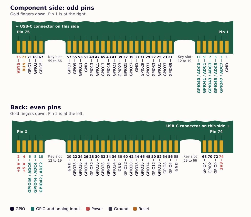
Every GPIO pin of the RP2350B, GPIO0 to GPIO47, has a pin of its own. GPIO40 to GPIO47 can also be analog inputs (ADC0 to ADC7).
| Pin | Component side | Pin | Back |
|---|---|---|---|
| 1 | GND | 2 | +5 V |
| 3 | GPIO47 (ADC7) | 4 | +5 V |
| 5 | GPIO45 (ADC5) | 6 | GPIO46 (ADC6) |
| 7 | GPIO43 (ADC3) | 8 | GPIO44 (ADC4) |
| 9 | GPIO41 (ADC1) | 10 | GPIO42 (ADC2) |
| 11 | GPIO40 (ADC0) | ||
| Key slot (12 to 19) | |||
| 20 | GND | ||
| 21 | GPIO39 | 22 | GPIO38 |
| 23 | GPIO37 | 24 | GPIO36 |
| 25 | GPIO35 | 26 | GPIO34 |
| 27 | GPIO33 | 28 | GPIO32 |
| 29 | GPIO31 | 30 | GPIO30 |
| 31 | GPIO29 | 32 | GPIO28 |
| 33 | GND | 34 | GPIO26 |
| 35 | GPIO27 | 36 | GPIO24 |
| 37 | GPIO25 | 38 | GND |
| 39 | GPIO23 | 40 | GPIO22 |
| 41 | GPIO21 | 42 | GPIO20 |
| 43 | GPIO19 | 44 | GPIO18 |
| 45 | GPIO17 | 46 | GPIO16 |
| 47 | GPIO15 | 48 | GPIO14 |
| 49 | GPIO13 | 50 | GPIO12 |
| 51 | GND | 52 | GPIO10 |
| 53 | GPIO11 | 54 | GPIO8 |
| 55 | GPIO9 | 56 | GPIO6 |
| 57 | GPIO7 | 58 | GND |
| Key slot (59 to 66) | |||
| 67 | GPIO5 | 68 | GPIO4 |
| 69 | GPIO3 | 70 | GPIO2 |
| 71 | GPIO1 | 72 | GPIO0 |
| 73 | RUN | 74 | 3V3 |
| 75 | VSYS |
The pins that are not GPIO pins:
- +5 V (pins 2 and 4): the power input from the carrier board.
- VSYS (pin 75): the supply of the board, from the USB-C connector or from the +5 V pins. The carrier board can take up to 0.5 A from it (Current from the VSYS pin).
- 3V3 (pin 74): the 3.3 V made on the board. The carrier board can take up to 100 mA from it (Current from the 3V3 pin).
- RUN (pin 73): the reset of the microcontroller. Connecting it to GND restarts the board, as the
RESETbutton does. - GND (pins 1, 20, 33, 38, 51 and 58).
What each GPIO pin can do
Each GPIO pin can be a plain input or output, or take one of the functions of the RP2350B: SPI, UART, I2C or PWM, and on some pins an analog input or another special function. The drawing shows the choices for every pin of the edge connector.
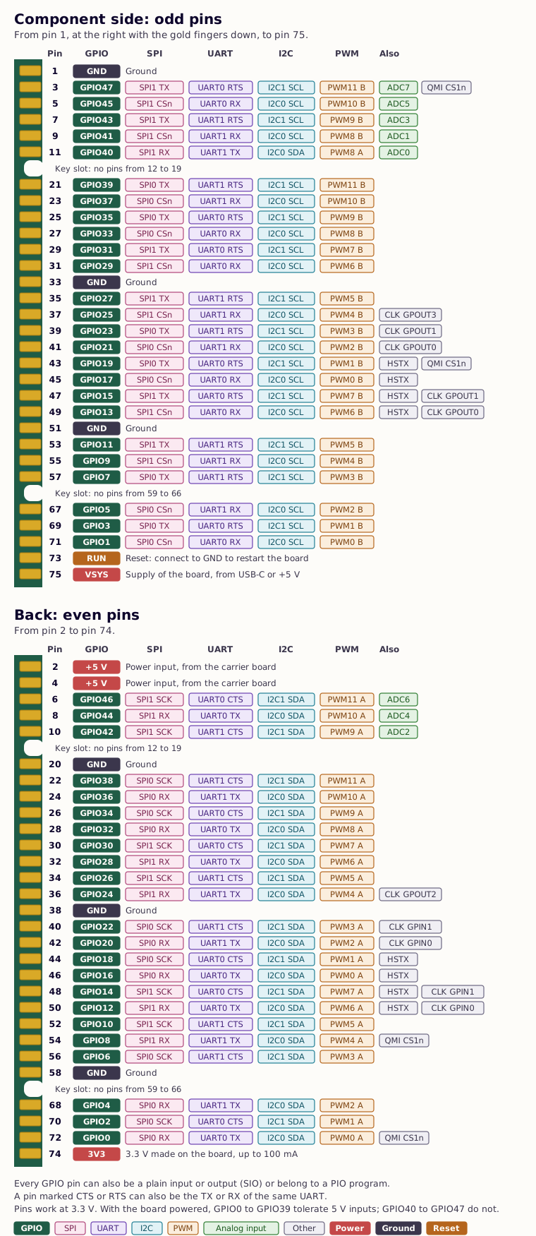
- SPI, UART and I2C: the RP2350B has two of each, numbered 0 and 1, and each one can be placed on several groups of pins. Choose pins of the same one: for example
SPI0 RX,SPI0 CSn,SPI0 SCKandSPI0 TX. - UART: a pin marked
CTSorRTScan also be theTXor theRXof the same UART. - PWM: twelve PWM generators,
PWM0toPWM11, each with two outputs,AandB. - Analog input:
ADC0toADC7, onGPIO40toGPIO47, with 12 bits and up to 500,000 samples per second. - HSTX: the high-speed transmit outputs of the RP2350B, on
GPIO12toGPIO19. - CLK: clock inputs (
GPIN) and clock outputs (GPOUT). - QMI CS1n: the chip select for a second memory chip on the bus of the flash memory.
- PIO: any GPIO pin can belong to a PIO program.
Voltage on the GPIO pins. Every GPIO pin works at 3.3 V. While the board is powered, GPIO0 to GPIO39 also accept inputs of up to 5.5 V. GPIO40 to GPIO47, the pins with an analog input, do not: never put more than 3.3 V on them. With the board unpowered, do not put more than 3.3 V on any pin.
On the versions with PSRAM, GPIO0 is the chip select of the PSRAM (QMI CS1n), which is why the board marks it GPIO0 (8MB CSn). Do not use GPIO0 for anything else on those versions.
The RP2350 datasheet from Raspberry Pi has the complete function table and the details of each function.
Buttons, pads and the LED
RESETrestarts the board.BOOTputs the board in BOOTSEL mode, to install a firmware: see below.- Red LED: lit while the board has power, from either input.
DEBUGpads, at the top right of the component side: the SWD signals of the RP2350B, for a debug probe. See The debug connector.D+andD-pads, on the back: the two data lines of the USB-C connector.
The debug connector
The DEBUG pads are made for the three-pin debug connector of Raspberry Pi, a three-pin JST-SH connector. The DBG connector version of the board has it fitted; on the other two versions the pads are bare (Versions).
It is fully compatible with the Raspberry Pi Debug Probe. Connect it to the D port of the probe with the cable that has a three-pin JST-SH connector at both ends, which comes with the probe.
Looking at the component side with the gold fingers down, the three signals are, from left to right:
| Pad | Signal |
|---|---|
| Left | SWCLK |
| Middle | GND |
| Right | SWDIO |
The two larger pads at the sides of the word DEBUG hold the connector in place and are connected to GND.
Installing a firmware
The RP2M2 takes its firmware as a .uf2 file over USB, with nothing else to install:
- Put the board in BOOTSEL mode. With the board unplugged, hold the
BOOTbutton, plug in the USB cable, then releaseBOOT. With the board already connected: press and holdRESET, press and holdBOOT, releaseRESET, then releaseBOOT. - A drive called
RP2350appears on your computer. - Copy the
.uf2file onto it. When the copy is complete the drive disappears and the board starts with the new firmware.
Which file to install depends on the product the board is part of. Each guide has the details, and the files to use have rp2350b in their name:
- TOS Emulator: Firmware installation
- Kickstart Multi ROM: Firmware installation
Products that use it
| Product | Computers | Guides |
|---|---|---|
| SidecarTridge TOS Emulator | Atari ST, STE, Mega ST and Mega STE | Board revision 4 |
| SidecarTridge Kickstart Multi ROM | Amiga 500, 500+, 600 and 2000 | Board revision 4 |
Both kits come with the RP2M2 16MB Flash, revision 1.4.0. The RP2M2 is not sold on its own: it comes as part of these kits.
In both, the RP2M2 plugs into the slot of a carrier board and is held with a screw. The carrier board is the part made for each computer: it fits the ROM sockets, and carries the green and orange LEDs and the RESCUE connector.
Coming soon
Breakout board for developers
We are working on a breakout board for the RP2M2, for developers who want to build and test their own designs with it. The RP2M2 plugs into the M.2 socket of the breakout board and is held with its screw, and the breakout board brings its pins out to screw terminals and pin headers.
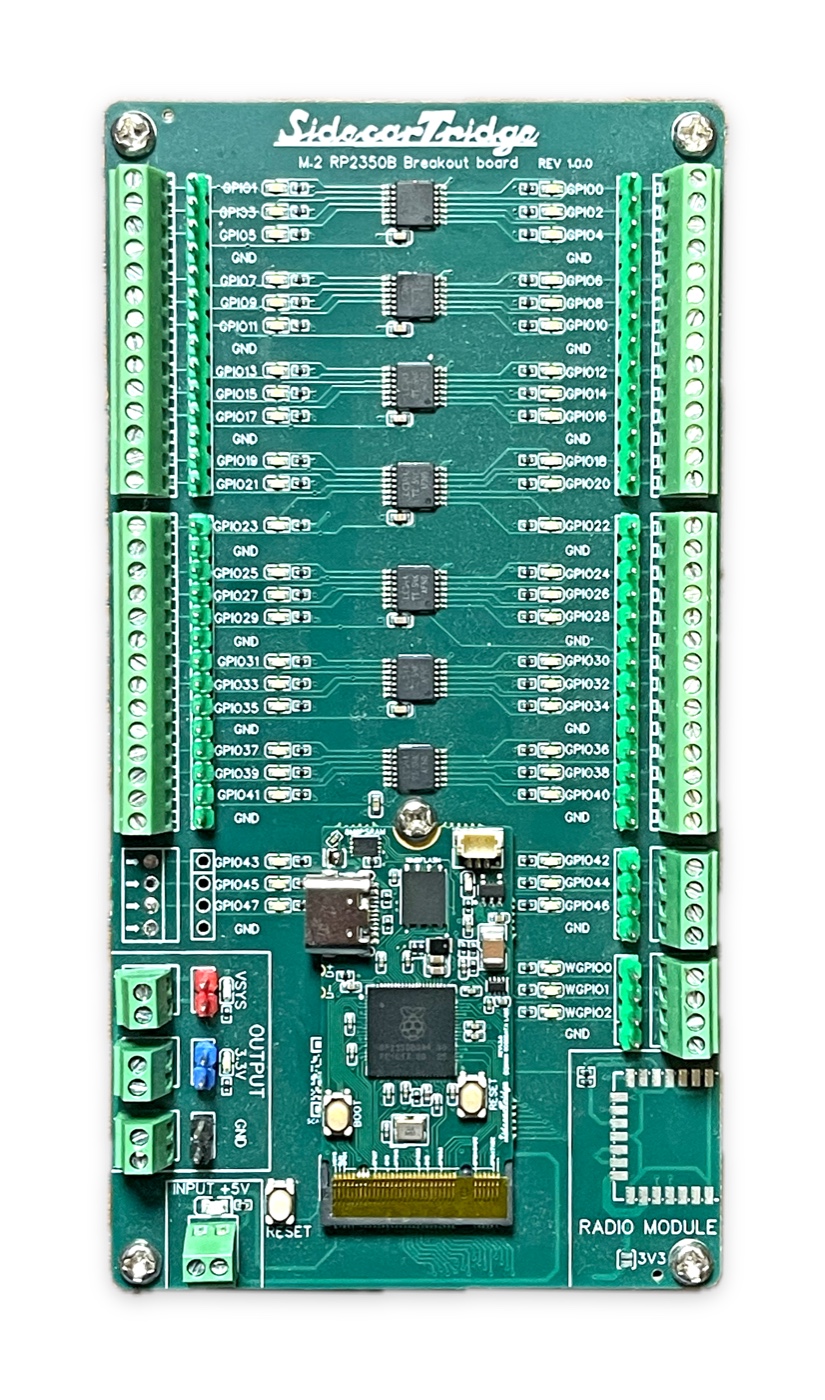
The prototype in the photo has:
- Screw terminals and pin headers for the GPIO pins of the RP2M2,
GPIO0toGPIO47, with GND terminals among them. - An LED for each GPIO pin.
- Power terminals: a +5 V input, and outputs for
VSYS, 3.3 V and GND. - A
RESETbutton.
The breakout board is still in development and is not on sale. The board in the photo is a prototype, and the final board may differ.
Links
- Quickstart: the QR code on the back of the board opens sidecartridge.com/quickstart, where you choose your product.
- Firmware files: the downloads page.
- Installing a firmware from the browser: webflash.sidecartridge.com.
- Declarations of conformity: Certifications.
- Support: write to us at support@gooddatalabs.com.